Electron Beam-Induced Current (EBIC) Analysis, as its name implies, is a semiconductor analysis technique that employs an electron beam to induce a current within a sample which may be used as a signal for generating images that depict characteristics of the sample, e.g., the locations of p-n junctions in the sample, the presence of local defects, and doping non-homogeneities. Since a scanning electron microscope (SEM) is a convenient source of electron beam for this purpose, most EBIC techniques are performed using a SEM.
When the primary electron beam of the SEM penetrates the semiconductor itself, holes and electrons that are free to move around are created by the impact. In a material that's free of any electric fields, these holes and electrons will be in random motion that allows them to find each other and recombine.
If electric fields within the semiconductor device do exist, however, these fields can influence the holes and electrons to move in a non-random manner, i.e., the holes and electrons will be separated and swept off to differently-charged areas. These electric fields may either come from external sources, or local to the sample such as those exhibited by p-n junctions.
With proper electrical contact with the sample, the movement of the holes and electrons generated by the SEM's electron beam can be collected, amplified, and analyzed, such that variations in the generation, drift, or recombination of these carriers can be displayed as variations of contrast in an EBIC image. EBIC imaging is very sensitive to electron-hole recombination, which is why EBIC analysis is very useful for finding defects that act as recombination centers in semiconductor materials.
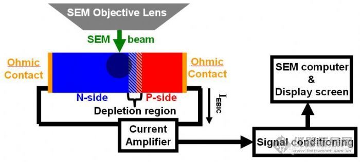
A typical EBIC system consists of the following: 1) a scanning electron microscope (SEM); 2) an external (i.e., located outside the SEM's high-vacuum chamber) low-noise current amplifier; 3) high-vacuum electrical feed-throughs that electrically connect the external current amplifier to the sample inside the SEM chamber; and 4) a sample holder with the required electrical contact points to facilitate the electrical connection of the sample to the feedthroughs.
The EBIC current (Iebic) collected is many times larger the primary beam current absorbed by the sample (Ib), and is given by the equation: Iebic = Ib x (Eb/Eeh) x n where Eb is the primary beam energy or the SEM's accelerating voltage EHT (on the order of several keV's), Eeh is the energy needed to create an electron-hole pair (about 3.6 eV for Si), and n is the collection efficiency. Thus, assuming a collection efficiency of 100%, and an EHT of 20 keV, the collected EBIC current would be about 5556 times that of Ib. EBIC currents are usually in the nanoampere to microampere range while Ib is in the picoampere range.
In areas of the p-n junction where physical defects exist, electron-hole recombination is enhanced, which reduces the collected current in those 'defect' areas. Thus, if the current through the junction is used to produce the EBIC image, the areas with physical defects will appear to be darker in the EBIC image than areas with no physical defects. EBIC imaging is therefore a convenient tool for finding sub-surface and other 'difficult-to-see' damage sites.
EBIC imaging is an effective analysis tool for bipolar circuits, but it is not effective in analyzing MOS circuits. This is due to the fact that the gate oxides of MOS transistors tend to trap charges from primary beam charge injection, resulting in false failures.
Applications of EBIC analysis include: 1) detection of crystal lattice defects, which show up as dark spots or lines; 2) location of p-n junction defects; 3) detection of collector pipes that result in collector-emitter leakage currents in bipolar transistors; 4) detection of extra junctions or doping layers; 5) identification of ESD/EOS failures sites; and 6) measurement of depletion layer widths and minority carrier diffusion lengths/lifetimes.