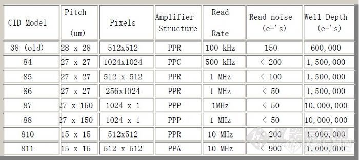
Charge Injection Device (CID) cameras have been in use since the early 1970's, but it has only been in the last several years that knowledge and experience have combined for a broader understanding of the technology and how to more fully apply it.
自从20世纪70年代CID电荷注入式设备检测器就已经被使用,但只是最近几年对其技术才有了更明确的理解以及怎样更全面的应用他的经验。
The CID concept was originated by scientists at General Electric Company working to devise a semiconductor memory chip. Exploiting the photosensitive characteristics of silicon, they developed a simple X,Y addressable array of photosensitive capacitor elements, and evolved the first CID camera in 1972. Development efforts continued through the 70's and 80's resulting in the generation of some 30 patents describing the basic structure and
readout techniques presently employed. CIDTEC was established when management took the business private through a leveraged buyout in July of 1987.
CID的概念最早是由通用电气公司设计半导体芯片的科学家们发明。采用Si的感光性特征,他们开发了一种简单的感光电容原理的X、Y(平面的)可设定地址的阵列,进而在1972年开发了第一个CID的相机。70年代和80年代不停的努力最终发明了现在采用的基本结构和读书技术的30多个专利。1987年7月通过杠杆买卖建立了CIDTEC这个公司。
Every pixel in a CID array can be individually addressed via electrical indexing of row and column electrodes. Unlike Charge Coupled Device (CCD) cameras which transfer collected charge out of the pixel during readout (and hence erase the image stored on the sensor), charge does not transfer from site to site in the CID array. Instead, a displacement current proportional to the stored signal charge is read when charge "packets" are shifted between capacitors within individually selected pixels. The displacement current is amplified, converted to a voltage, and fed to the outside world as part of a composite video signal or digitized signal. Readout is non-destructive because the charge remains intact in the pixel after the signal level has been determined. To clear the array for new frame integration, the row and column electrodes in each pixel are momentarily switched to ground releasing, or "injecting" the charge into the substrate.
CID阵列上的每个像素可以单独通过行列电极的电子标定指数来寻址。不像CCD(电荷耦合式设备)在读书的时候会将像素中收集的电荷转移,电荷不会在CID阵列的点到点转移。在电荷信息包在独立所选择的像素中的电容之间移动的时候,和所存储的信息电荷成正比的移位电流被读取。移位电流被放大,转换成为电压,作为部分复合视频信号或者数字信号输送给外部世界。由于信号电平被测定以后电荷完整无缺的保留在像素中,所以其读书是非破坏性的。要对新的帧进行几分而清除阵列,每个像素上的行和列电极就会即可切换到接地释放,或者“注射”电荷到底层。
This principle of operation makes CID technology fundamentally different from other imaging techniques, giving rise to a number of technical advantages that can be used to solve imaging problems. For instance, the nondestructive readout capability of CID cameras makes it possible to introduce a high degree of exposure control to low-light viewing of static scenes. By suspending the charge injection, the user initiates "multiple-frame integration" (time-lapse exposure) and can view the image until theoptimum exposure develops. Integration may proceed for milliseconds or up to several hours with the addition of sensor cooling, applied to retard accumulation of thermally-generated dark current. Controlled integration is useful for scientific and photographic applications, especially in astronomy.
这种操作原理是的CID技术根本不同于其他成像技术,具有许多可以解决成像问题的技术优点。例如,CID照相机的非破坏性读书能力使得其可以传入高度曝光控制到静物的低光度观察。通过悬置电荷注射,使用者可以初始化多帧积分(延时曝光)同时能够在找到最佳曝光的时候再来观看图像。积分可以从毫秒高到几个小时(此时需要额外冷却检测器用来阻止有热所产生的)
暗电流的累积)。控制积分对于科学和照相应用特别是天文学非常有用。
At brighter intensities, "blooming" and "smearing" describe the distortion in an image that can occur when solid-state video cameras are exposed to concentrated, non-uniform light as in the images below.
对于较明亮的光强,溢出和托尾效应讲的就是图像的扭曲,在固态视频照相机受到集中的、非一致的光的照射的时候。
![]()