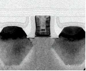
新人一个,对半导体一窍不通。。。有没有大虾给讲解下。。就知道这个是45nm PMOS, 但什么是什么一点摸不清。。。
- STI, well, and VT implants,
- ALD (18-20Å) of HK gate dielectric,
- polysilicon deposition and gate patterning,
- source/drain extensions, spacer, Si recess and SiGe deposition,
- source/drain anneal, Ni salicidation, ILD0 deposition,
- poly opening CMP, poly removal,
- pMOS work-function metal deposition,
- metal gate patterning, nMOS workfunction metal deposition, and
- metal gate Al fill and Al CMP, etch-stop layer deposition.
![]()